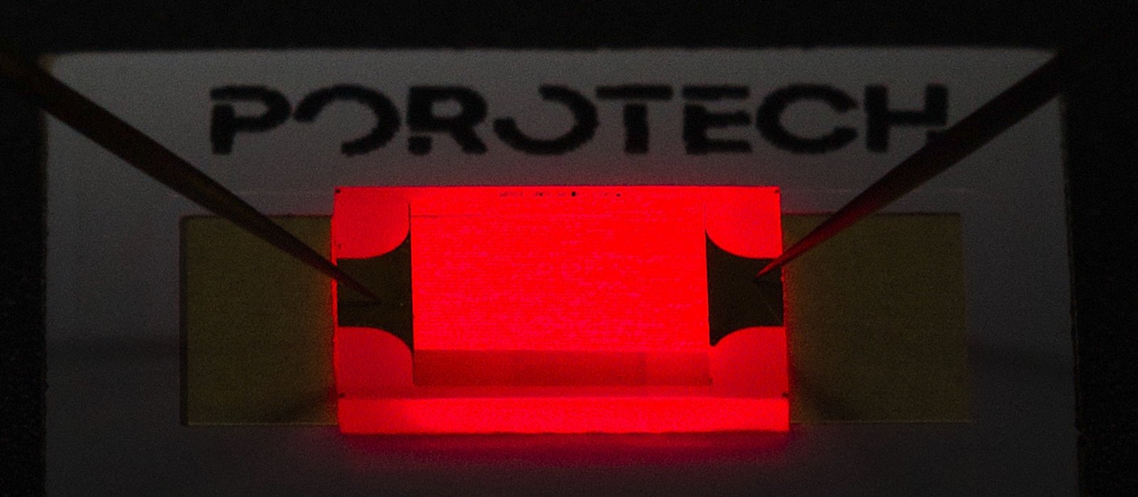
Porotech, a University of Cambridge spin-out, has raised £3 million in its drive to fuel the next generation of micro-LED production. The startup has pioneered a revolutionary new class of porous gallium nitride (GaN) semiconductor material, one that paves the way for brighter, sharper, and more vivid microdisplays. And this author, on a sunny day, thanks them for it. To date, the company has raised £4.5 million.
While you’ve most probably heard ad nauseam about silicon, I’m going to go out on a limb and take a wild guess that gallium nitride hasn’t quite made it to the dinner table conversation. In a nutshell, gallium nitride is the new silicon.
One of the properties of silicon that makes (made?) it so attractive to semiconductor manufacturers is what’s known as a “band gap”. Every material under the sun has a band gap, or how well it can conduct electricity. GaN, a transparent, glass-like material, has a wider band gap than silicon, meaning it can sustain more juice than a similar sample of silicon can survive.
What Porotech has done, and the hint is in the name, is developed a manufacturing method whereby, “Porous GaN is basically GaN with tiny holes in it that are a few tens of nanometres across," says Porotech CEO and co-founder Dr. Tongtong Zhu. "It's an entirely new engineered GaN material platform to build semiconductor devices on. It offers performance improvements that are suitable for mass production, scalable in wafer size – and crucial for the next generation of microdisplay devices.”
If you’re still with me up to this point, but are wondering, “what the heck is a microdisplay device?” I point to your smartwatch, your phone, and, here’s where the gamechanger might come into play, AR/VR devices.
The struggle with current methods arrives with the convergence of aluminium indium gallium phosphide (that’s a lot of ‘um’s, so let’s just call it AIInGaP) and quantum dot colour conversion (QDCC). AIInGaP and QDCC (lmnopqrstuv) have a hard time dealing with the small pixel sizes required by AR on the AIInGaP side, and uniformity and stability issues on the QDCC side.
Porotech is taking this on by allowing all three primary colours to be made with the same GaN material and integrated into a single wafer. The company reports being able to deliver these porous GaN substrates and micro-LED epiwafers on sapphire and silicon platforms ranging from 100mm (4") to 300mm (12"). Small AND stable? Where do I sign up?
While the company was founded in 2018, it’s only spun out of Cambridge in January of 2020. and has not only been generating revenue for the past 10 months but attracted the interest of some of the biggest names in display technology. And if we're talking AR/VR displays, your author has to throw the words Samsung and Apple out on the table. Representatives from Porotech declined to comment.
Porotech’s raise was led by Speedinvest and saw participation from previous investors IQ Capital, Cambridge Enterprise, Martlet Capital, and Cambridge Angels.
"This new type of porous GaN semiconductor material fits within existing industry processes and is robust and flexible enough to be tailored to different applications. Porotech has demonstrated that it has both the product and the commercial capability to become a key player in next-generation display technology," concludes Speedinvest’s Rick Hao.


Would you like to write the first comment?
Login to post comments