

Invisix, a semiconductor metrology company developing next-generation measurement tools for advanced chip manufacturing, has raised an oversubscribed €20 million seed round. The financing includes participation from Hitachi Ventures, Transition Ventures, imec.xpand, Doosan Investment Co., and a tier-one semiconductor manufacturer.
As semiconductor devices become smaller and more complex, measuring the critical structures inside advanced chips is becoming increasingly difficult. Manufacturers must verify each layer before adding the next, yet conventional optical metrology tools can no longer resolve many of the buried features that determine device performance. As these chips power high-performance computing and AI, demand is growing for faster, non-destructive measurement solutions that can improve yields and accelerate production.
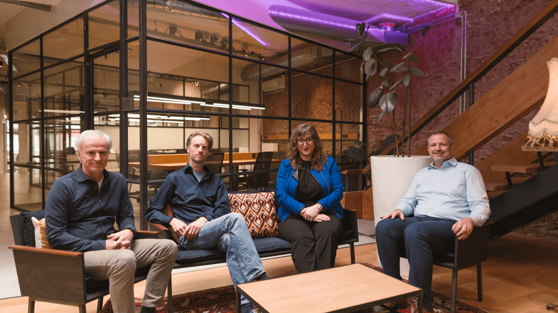
Founded by ASML alumni and PhD physicists Christina Porter and Sietse van der Post, Invisix is developing a soft x-ray metrology platform designed to enable high-volume, non-destructive measurement of some of the most challenging semiconductor structures.
According to Christina Porter, PhD, co-founder and CEO of Invisix, the growing complexity and three-dimensional nature of advanced semiconductors is driving demand for a new generation of metrology tools capable of inspecting critical internal structures without damaging devices.
We are entering the market with technology that has been incubated inside ASML for more than a decade — a level of technical de-risking that is unusual for a seed-stage hardware company and gives our customers a faster path to deployment.
The company's technology is based on High Harmonic Generation (HHG), a process rooted in scientific discoveries recognised by the 2023 Nobel Prize in Physics. HHG uses a short-pulsed laser to excite noble-gas atoms into a high-energy state, causing them to emit soft x-rays across multiple wavelengths. This generates a richer three-dimensional signal than conventional single-wavelength laser systems.
By combining HHG with proprietary reconstruction algorithms and machine learning, Invisix reconstructs detailed three-dimensional images of internal device structures without damaging the wafer. The system architecture has also been designed to deliver the throughput required for high-volume semiconductor manufacturing.
Invisix applies to metrology the same principle that transformed semiconductor lithography: as device dimensions shrink, the wavelength used to measure them must shrink as well. By using soft x-rays, the company aims to provide visibility into buried nanoscale structures that are increasingly inaccessible to conventional optical inspection methods.
The technology has already been validated through industry collaborations, including work with Intel and imec, and the company continues customer demonstrations from its new Eindhoven cleanroom facility. Invisix is now focused on bringing its first commercial system to market and enabling semiconductor manufacturers to measure the next generation of advanced devices at production scale.
The funding will be used to expand the Invisix team, accelerate development of its first commercial system, and support customer demonstrations at the company's new cleanroom facility in Eindhoven.


Would you like to write the first comment?
Login to post comments